Lab 7: The Advanced Encryption Standard
Number of Hours Spent on Lab: 25 hours
Main Goals
The main goal of this lab was to build a system on an FPGA that can fit on the chip. An interface was also designed and implemented to allow for communication betweent the FPGA and MCU. Finally, a hardware accelerator was created to perform 128-bit AES encryption where a plaintext message key was being sent from the MCU to the accelerator and back.
Design Approach
AES Encryption Design
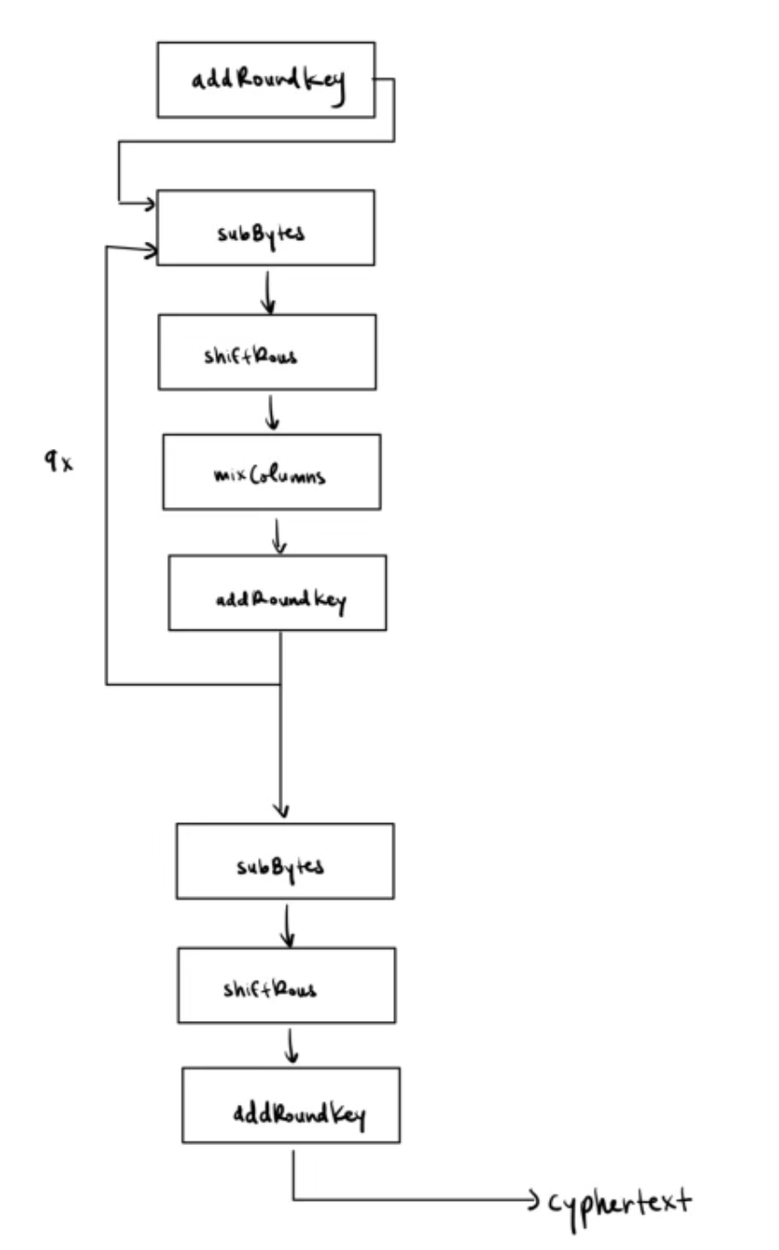
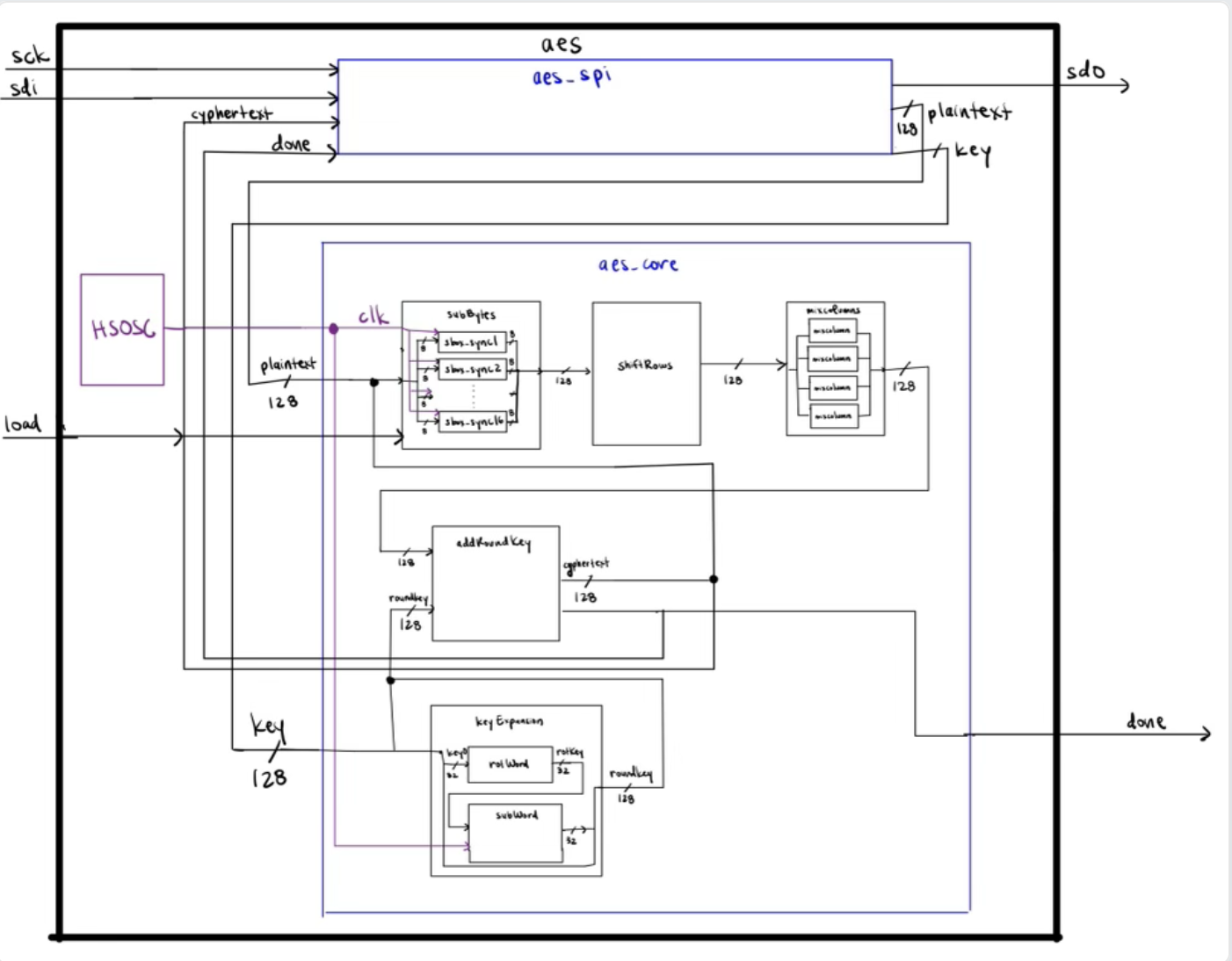
In order to create subBytes, sbox_sync was used to alter the input bits. Sbox_sync was used instead of sbox in order to store the LUT in RAM memory since a 16x16 would have been too large to store within our local memory. Sbox_sync was then called 16x on the 8 different rows of bytes of plaintext inputted to it, and allowed SubBytes to then output the 128 bits of modified text which was then fed into the shiftRows, mixColumns, and addRoundKey. In order to create the subModule keyExpansion, submodules rotWord and subWord were used to correctly output the roundKey values. These values were then also passed into addRoundkey to get the new cyphertext and into keyExpansion to get the new set of roundKey values. The design ensured that the modules would would go through the four submodules for a total of 9 times, only go through subByte, shiftRows, and addRoundKey for the 10th time, and then output the cyphertext. Below shows the path of the 128-bit AES encryption path and the Block Diagram of the modules used to implement this.
FSM Design
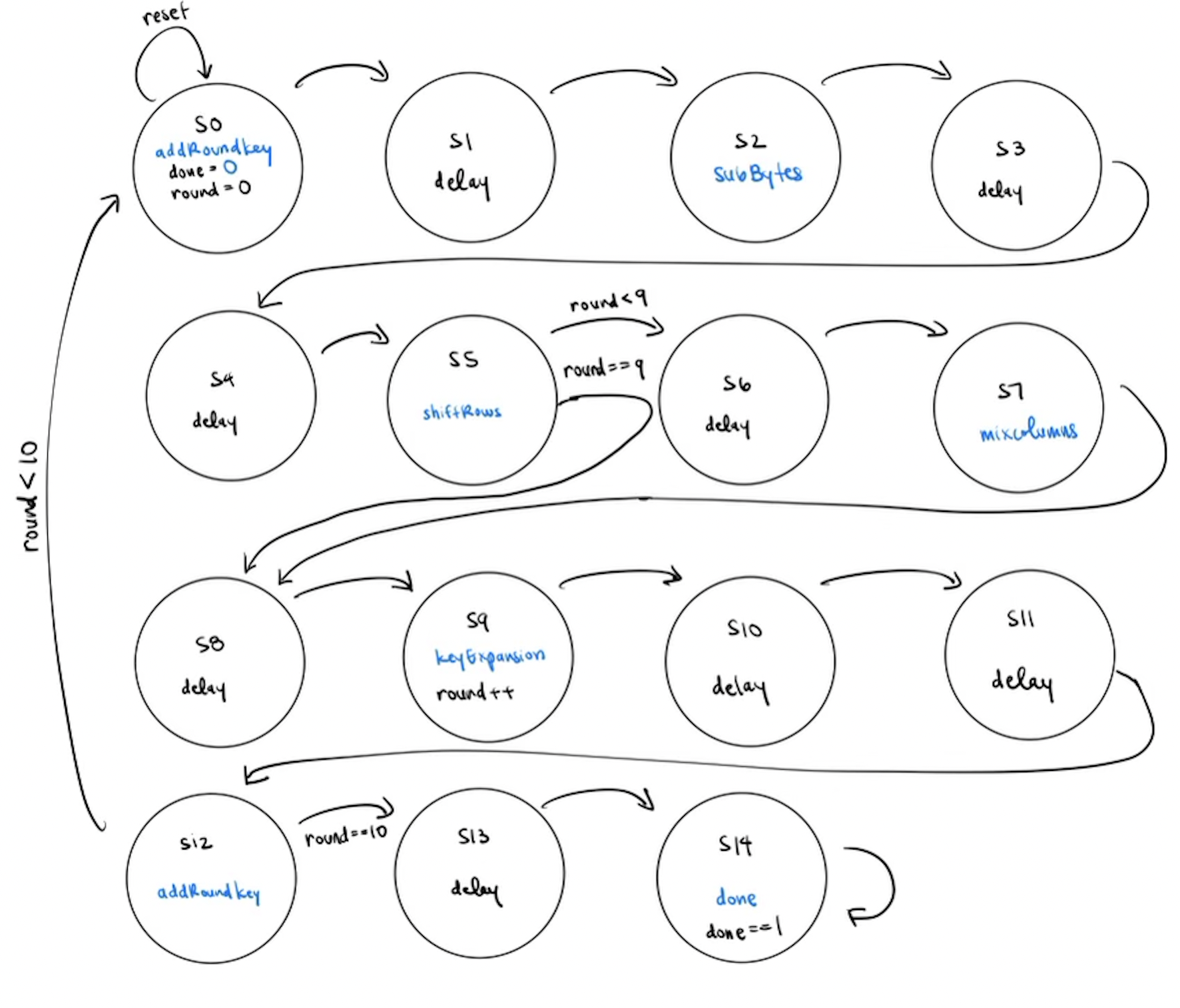
In order to connect the submodules for the Encryption Design, an FSM was designed to determine what information should be passed to the AES submodules during each clock cycle. It was also used to determine the number of rounds the cyphertext had been encrypted, so that it would know when it is done. A delay was implemented between each submodule in the form of an extra state to take into account any clock delays from calling sbox_sync in keyExpansion and subByte.
Pin Assignment
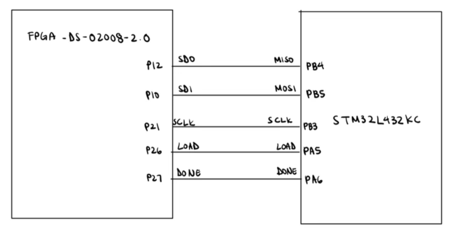
| FPGA | pin # |
|---|---|
| SDO | 12 |
| SDI | 10 |
| SCLK | 21 |
| LOAD | 26 |
| DONE | 27 |
| MCU | pin # |
|---|---|
| MISO | B4 |
| MOSI | B5 |
| SCLK | B3 |
| LOAD | A5 |
| DONE | A6 |
Testing Approach
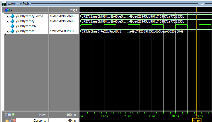
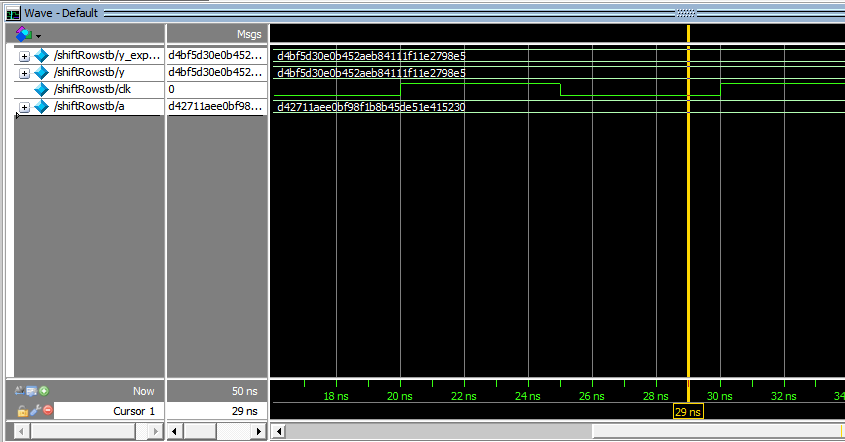
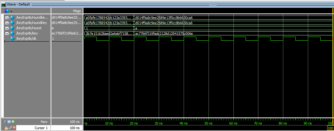
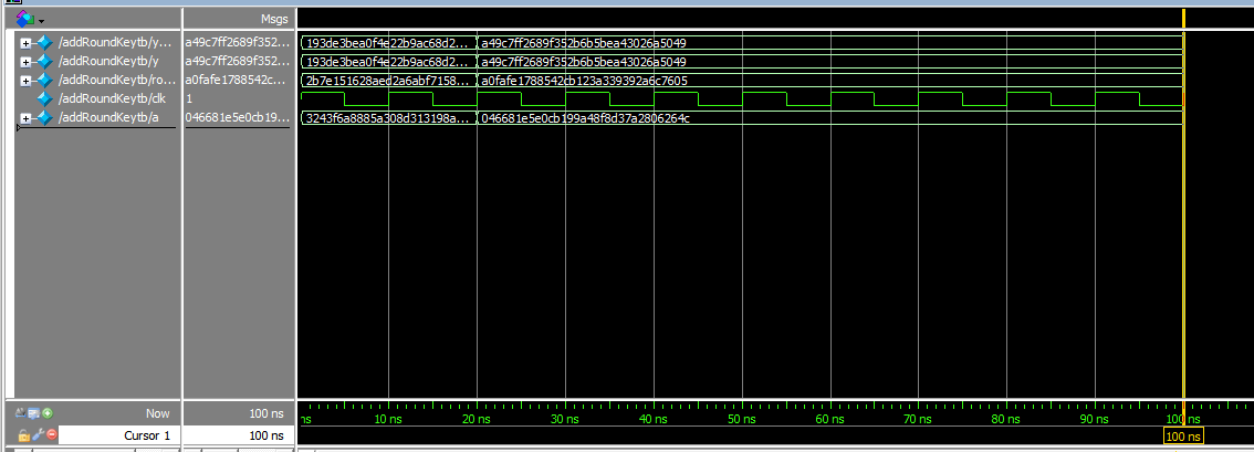
In order to test the design, the System Verilog code was opened in ModelSim. A set of additional testbench files in System Verilog were created to test each of the submodules’s functionality.
The subByte module, shiftRows module, keyExpansion module, and addRoundkey module were tested individually with known inputs and outputs. Once all of waveforms outputted matched the expected, a testbench for aes_core was then used to test the FSM design. As you can see below, the outputs of the aes_core testbench and aes_spi testbench were successful because it returned the expected values.


Design Requirements
After testing the design in ModelSim, I can confirm the design meets all specs.