Lab 3: Keypad Scanner
Number of Hours Spent on Lab: 30 hours
Main Goals
The main goals of this lab were to use design and implement and circuit interface on the FPGA that read a keypad matrix. This required creating a solution to address issues that arose from switch bouncing. Finally, the last 2 inputted digits needed to be displayed on a pair of 7 segment LED displays.
Design Approach
FSM Design
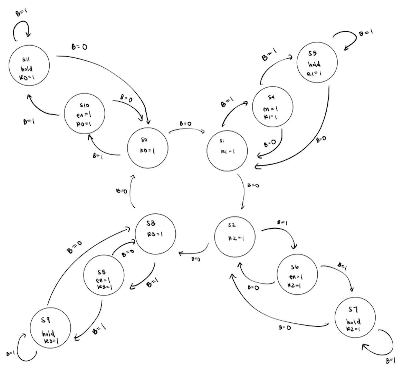
In order to detect which row and column were turned on during a button pressed, all of the rows could not be turned on at once because then several keys would be viewed as on with a single button press. Thus, the idea was to scan through the rows during each clock cycle, and then take the columns as an input to the FPGA. Whenever a column is detected on, the FPGA can then figure out which row was powered on that time and then decode the corresponding key value.
An FSM was created to keep track of all of the states. States 0, 1, 2, and 3 are cycled through when the button is off, until a button is turned on. The button is turned on when any of the column inputs are detected to be on. When a button is turned on, the next state will be a separate state (represented by States 4, 6, 8, 10) that will be stayed at for one clock cycle. The enable is represented when any of these states are turned on, because it will be used later to track when the digits on the keypad need to be shifted. Finally, after the button is pressed, if it is still being pressed or held down after the first clock cycle, it will be moved to a holding state represented by States 5, 7, 9, and 11. In addition, only one button click should be detected, which is why these states exist, and the program will stay on these states until the button is turned off.
| Current State |
|---|
| S0 |
| S1 |
| S2 |
| S3 |
| S4 |
| S5 |
| S6 |
| S7 |
| S8 |
| S9 |
| S10 |
| S11 |
| B = 1 | B = 0 |
|---|---|
| S10 | S1 |
| S4 | S2 |
| S6 | S3 |
| S8 | S0 |
| S5 | S1 |
| S5 | S1 |
| S7 | S2 |
| S7 | S2 |
| S9 | S3 |
| S9 | S3 |
| S11 | S0 |
| S11 | S0 |
| B = 1 | |
|---|---|
| R0 = 1 | |
| R1 = 1 | |
| R2 = 1 | |
| R3 = 1 | |
| R1 = 1 | en = 1 |
| R1 = 1 | |
| R2 = 1 | en = 1 |
| R2 = 1 | |
| R3 = 1 | en = 1 |
| R3 = 1 | |
| R0 = 1 | en = 1 |
| R0 = 1 |
//See Table 1 for details, especially Table 1 (c).
System Verilog Design
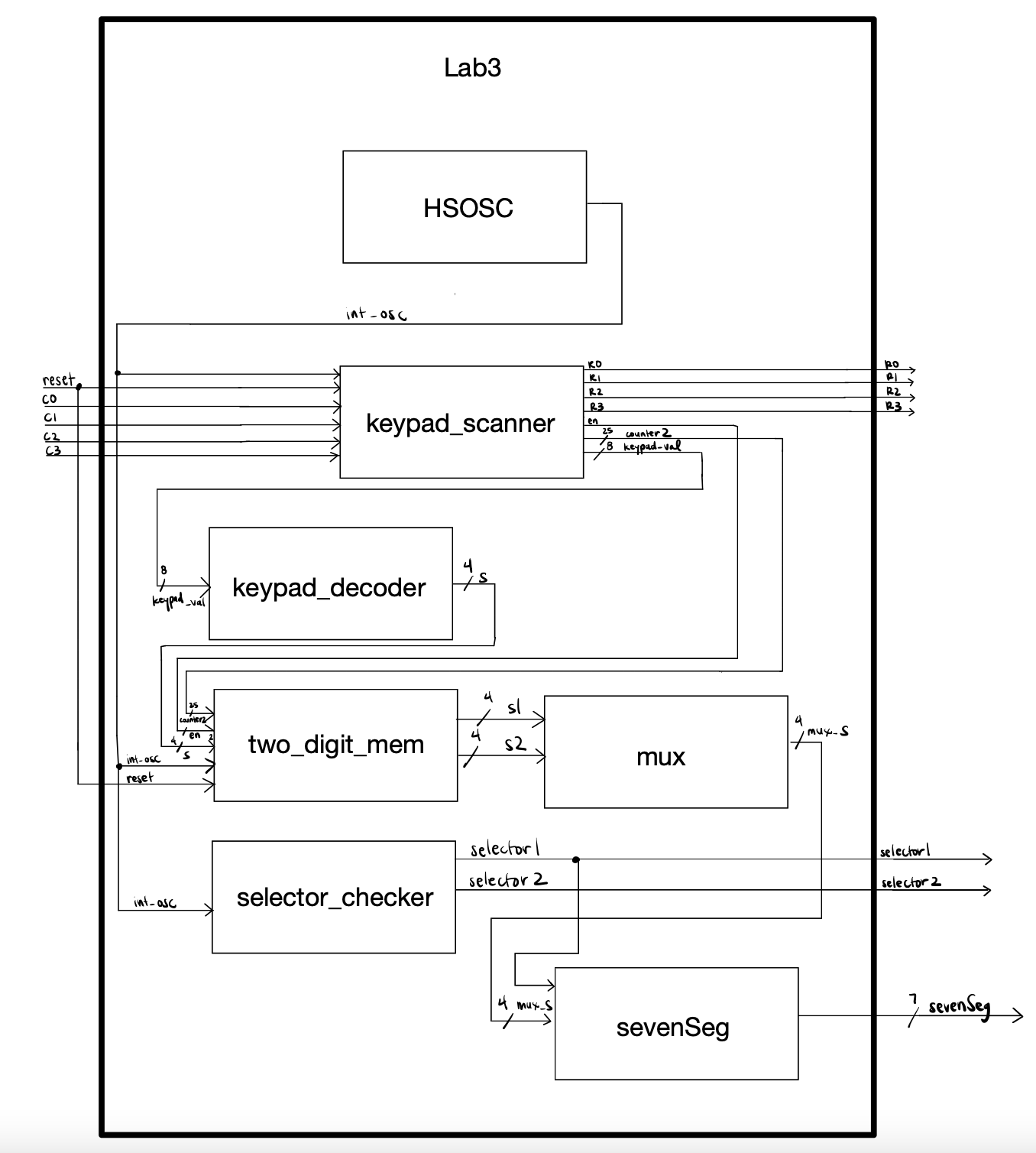
The System Verilog code created consisted of an internal high speed oscillator at 2.4kHz, so that the values displayed on the LED are going fast enough that it looks like the values are being displayed simultaneously. This same clock was also used for the keypad_scanner, two_digit_mem, and selector_checker.
The keypad_scanner submodule took in the column inputs of the physical keypad and outputted an 8 bit value that represented which rows and columns were turned on at each clock cycle. A counter was also outputted that counted for 50 clock cycles to represent what values should count as an actual button press as opposed to switch bouncing. Finally, an enable was also outputted that represented when each button was turned in the form of one clock cycle.
The 8 bit value outputted from the keypad_scanner was then inputted to another submodule known as keypad_decoder taht return a 4 bit value representing the desired hex value that should be displayed on the seven segment display.
In order to shift the key values properly to display the last 2 values pressed on the keypad, a shifting submodule was created. This submodule would shift the key values at every clock edge only if the enable was high (button is on for exactly one clock cycle) and if the counter was greater than 50 clock cycles. This ensured that there was no switch bouncing and also that the the keypad values were be shifted for only one clock cycle. This submodule would then output the two desired hex values that should be displayed on the seven segment display.
System Verilog code for how the two values were displayed on the sevenSeg were used from Lab 2.
7 Segment and Transistor Circuit Design
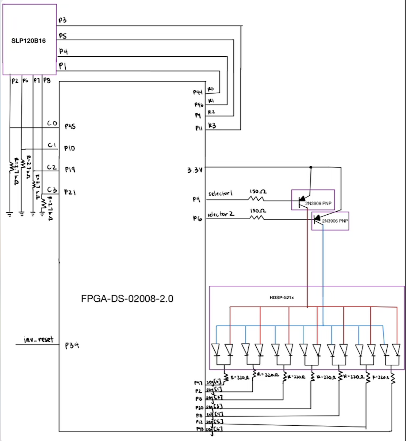
Since there are 2 segments that will be alternating between two digits with the same set of FPGA pins, a transistor was needed to control whether each of the digits should display an LED value or if it should be turned off completely. Since the LED display used was a common anode, we could connect a PNP transistor to drive the common anode’s current to high when it is on or low when it is off. For the display, that means pins 13 and 14 were each connected to their own transistor’s output. I then connected both of the LED segments respective outputs to the same FPGA pins. The various pins that controlled the display were connected to the FPGA board using 220 Ohm resistors in order to achieve 7 mA of current.
Keypad Circuit Design
The keypad consisted of 8 pins that powered the 4 rows and 4 columns. The 4 column were connected as inputs to the FPGA. They all required pull-down resistor values in order to ensure that the input was not floating. This resistor value was calculated in order to minimize the current flow to about 1.2 mA. As a result, the resistors used for the circuit are all 2.7 kOhms.

In addition, the 4 pins connected to the rows of the keypad acted as direct inputs to the FPGA.
Pin Assignment
Finally, the pins from the FPGA needed to be correctly assigned to the 7-segment display and keypad pins. The column variables (C0, C1, C2, C3), reset, row variables (R0, R1, R2, R3), selectors, and 7 segment values (seg) defined in System Verilog were assigned to physical pins on the board shown as the following:
| variable | pin # |
|---|---|
| seg[0] | 47 |
| seg[1] | 2 |
| seg[2] | 13 |
| seg[3] | 20 |
| seg[4] | 18 |
| seg[5] | 12 |
| seg[6] | 48 |
| selector1 | 6 |
| selector2 | 4 |
| C0 | 45 |
| C1 | 10 |
| C2 | 19 |
| C3 | 21 |
| R0 | 44 |
| R1 | 46 |
| R2 | 9 |
| R3 | 11 |
| reset | 34 |
Tradeoffs of Chosen Design
The design I created involved creating a lot of modules for each of the design’s functions. This made it easy for me to test and debug each module individually, and also understand the process flow of the circuit design. However, when I was testing the modules all together, I had a lot of difficulty tracking down which module the issue would arise in because there were a lot of internal variables being passed through each module.
Another design choice I made was the FSM design. The FSM design was intuitive because it used a lot of the concepts we used in class such as how to get a pulse for only one clock cycle. I also understood what was happening the FSM, so it was easier for me to implement in System Verilog. However, when I was trying to implement debouncing later, it was difficult to do so within the existing FSM, since that FSM was already fully set. Thus, I was trying to create a debouncing system that did not affect or further complicate the current FSM implemented. This definitely caused some difficulty because of the design constraints.
Testing Approach
In order to test the design, the System Verilog code was opened in ModelSim. A set of additional testbench files in System Verilog were created to test each of the submodules’s functionality.
Keypad Scanner Testing
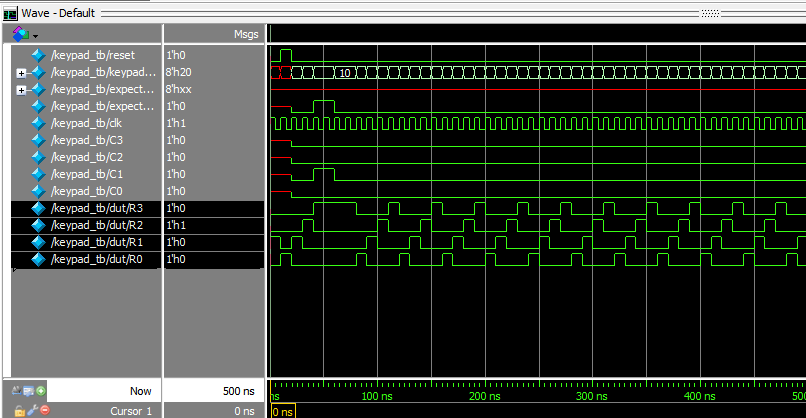
In order to check if the oscillator function was working properly, a clock signal was generated with 10 timesteps. A dut (device under test) was then instantiated calling the oscillator function. The testbench was then run for 2000 ns. At random times, one of the column inputs would be forced to 1. When looking at the output of the testbench in the Wave view, it shows the rows rotating on high every clock cycle until a column is turned on high. When the column is high, the value of the row it is set on will stay high as expected. Thus, the keypad_val outputting at this point is a combination of the columns and rows that are high.
Keypad Decoder Testing
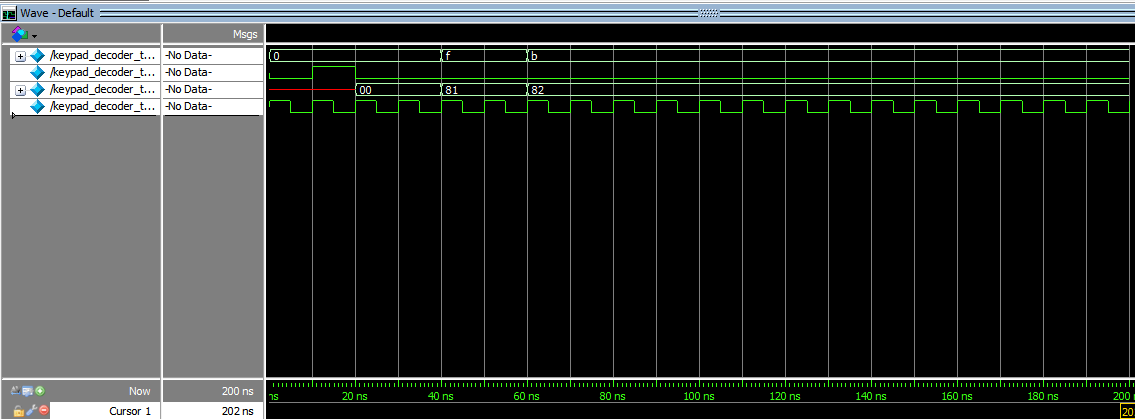
In order to check if the keypad decoder function was working properly, a clock signal was generated with 10 timestep. A dut (device under test) was then instantiated calling the keypad decoder function. At the start of the simulation, input values for the keypad decoder reflecting which rows and columns were currently on. The waveforms could then be observed of the output to ensure it shows the expected binary output based on the row and column inputs.
Two Digit Memory Testing
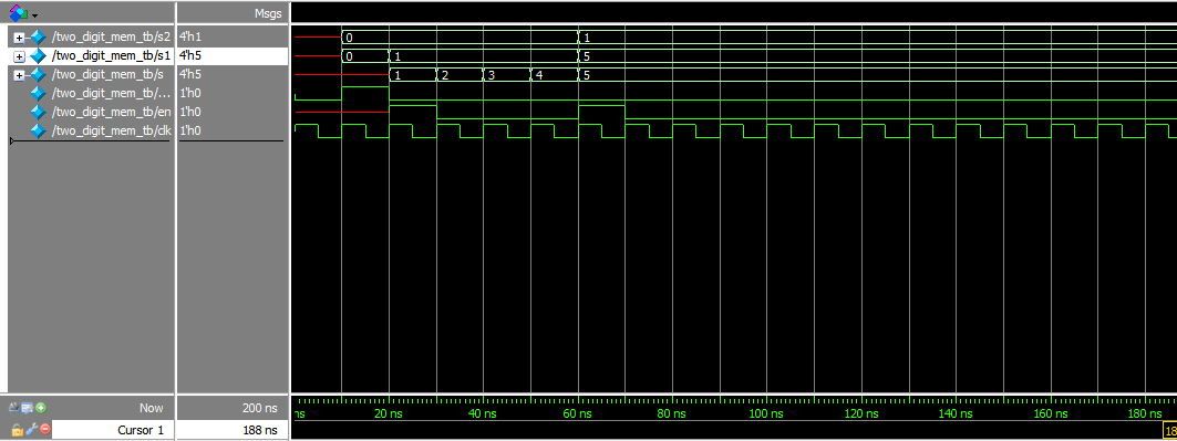
In order to check if the two digit memory function was working properly, a clock signal was generated with 10 timestep. A dut (device under test) was then instantiated calling the two digit memory function. At the start of the simulation, input values for the input switch were set to various values. Some were held for less than 50 clock cycles, while others were held for longer than 50 clock cycles. The two digit memory was supposed to take care of switch bouncing, so the waveform should show the output s1 and s2 values only capturing and switching values when the input s is held for longer than 50 clock cycles. This behavior was observed in the waveforms. Thus, the module behaved as expected.
Top Module
Before transferring all of the code to Radiant Software, a final testbench was created for the top module that tested all of the submodules together. A dut was instantiated with the column inputs and expected output being held at various values. At one point, one of the column inputs were held for less than 50 clock cycles to test switch bouncing. The output of this waveform was the expected seven Segment output pins in binary. In the waveform, it can be seen that there are two values oscillating as expected to reflect the keypad input simulated.
