Lab 1: FPGA and MCU Setup and Testing
Number of Hours Spent on Lab: 14 hours
Main Goals
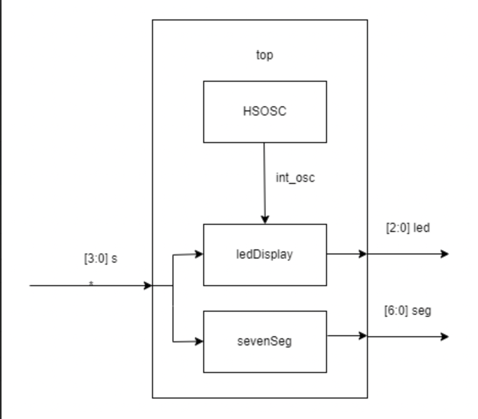
The main goals of this lab was to assemble the development board and test out the MCU and FPGA boards. In addition, an FPGA design was created in System Verilog to control 3 LEDs on the board and a 7-segement display. The LEDs and 7-segement display behavior is based on input of the switches on the board. As a result, the 7-segment display needed to be interfaced to the FPGA board in order to work as desired.
Design Approach
LED Design
In order to design the project so that the LEDs worked properly, I recognized that one of the led[1] is controlled by an AND gate and the second led[0] is controlled by an XOR gate of the switch values. Led[2] needed to blink at 2.4 Hz using an internal high-speed oscillator. By using the starter code provided in the fpga_dev_board_test file, a new maximum counter value needed to be calculated. Since the internal oscillator is running at 48 MHz, we get the number of counts to be 10M to get an led blinking at 2.4 MHz assuming we want a 50% duty cycle. An additional variable needed to be created in order to check if the led should be turned on or off every time the counter gets to 10M.

7 Segment Display Design
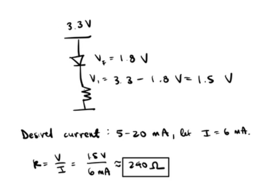
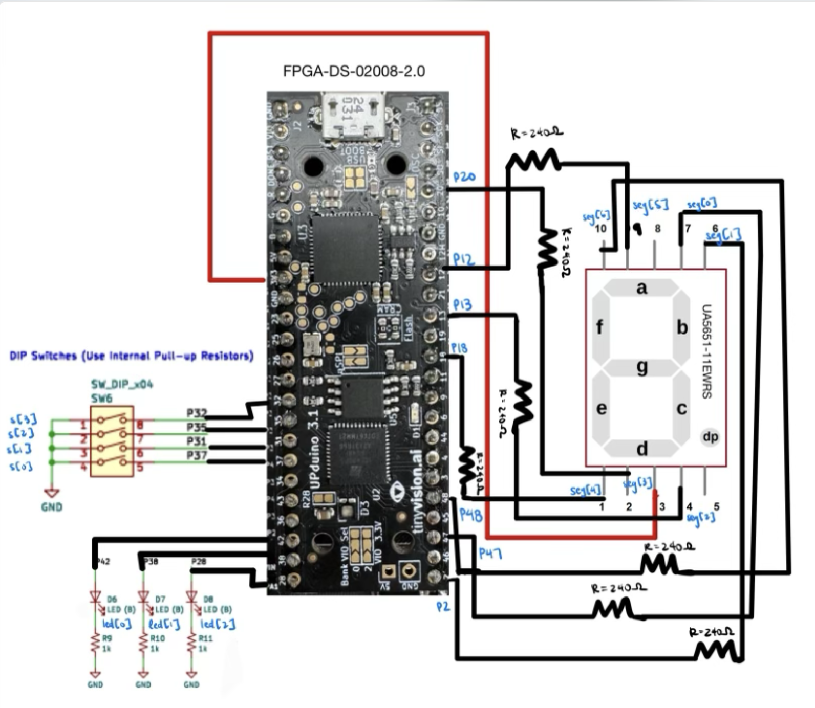
In order to design the 7-segment display, I had to use a series of case statement for the 16 different outputs to be displayed based on the switches in a separate submodule. It was important to set pin 3 on the display to the 3.3 V so that it is always on. Thus, the segement’s cathode will turn the segement on when it is set to 0. Each case statement set the output segement values to 0 when that segement should be turned on based on what binary value was currently set on the input switches. This code was written in a separate file but was called in the same file that controlled the 3 Leds. In order to wire the 7-segment display, the various pins that controlled the display were connected to the FPGA board using 240 Ohm resistors in order to achieve 10 mA of current.


Pin Assignment
Finally, the pins from the FPGA needed to be correctly assigned to the switches, Leds, and 7-segment display on the board. The s, seg, and led variables defined in System Verilog were assigned to physical pins on the board shown as the following:
| variable | pin # |
|---|---|
| s[0] | 37 |
| s[1] | 31 |
| s[2] | 35 |
| s[3] | 32 |
| led[0] | 42 |
| led[1] | 38 |
| led[2] | 28 |
| seg[0] | 47 |
| seg[1] | 2 |
| seg[2] | 13 |
| seg[3] | 20 |
| seg[4] | 18 |
| seg[5] | 12 |
| seg[6] | 48 |

Testing Approach
In order to test the design, the System Verilog code was opened in ModelSim. The values of input s can be forced to any binary combination, and the output from the code could be seen in the Wave view. Upon doing so, I could see that the output I was receving from the forced inputs were the desired values. A testbench was also created to check that there were no errors in my logic.
Finally, I uploaded the code to my FPGA board, which was also connected to the 7-segment display through a ribbon cable. After toggling with the physical input switches, the desired led behavior and 7-segment display was shown. I also used an oscilloscope to measure the frequency of the third led to ensure it had the desired frequency of 2.4 Hz.

Design Requirements
After testing the design on both ModelSim and physically, I can confirm that it meets all the requirements.